Explore materials at the microscopic level with the Scanning Electron Microscopy microcredential, April 24 and May 1
Ever wondered how engineers analyze materials at the microscopic scale?
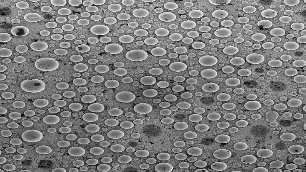
The Materials Characterization with Scanning Electron Microscopy, or SEM, microcredential gives you hands-on experience with one of the most powerful tools used in modern engineering and manufacturing.
In this 10-hour program, you’ll learn how to operate a benchtop SEM and explore how materials behave under high-resolution imaging. Through guided lab sessions, you will:
- Understand the physics behind SEM.
- Prepare samples for metals, polymers and ceramics.
- Capture and interpret high-quality SEM images.
- Evaluate material structure and properties.
This course is ideal for students interested in materials science, semiconductor technologies and advanced manufacturing.
Friday April 24, 2026 and Friday, May 1, 2026
1–6 PM
Interdisciplinary Science and Technology Building 12 (ISTB12), Polytechnic campus [map]
Register now
The fee is $25 for ASU students.
You’ll leave with practical lab experience and skills that are directly applicable in research and industry environments, as well as a digital microcredential from ASU, helping demonstrate your skills to future employers.